
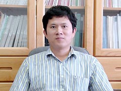
學歷
- 美國明尼蘇達大學 資訊科學博士
經歷
- 美國IBM大型電腦系統發展中心開發研究員
- 大同工學院資訊科技應用研究中心副研究員
- 元智大學資工系主任(2011~2017)
- 元智大學資訊學院英語學士班主任(2018~2022)
教授課程
- 資訊概論(Introduction to Computer Science)
- 程式設計實習(C++) (Computer Programming Lab, C++)
- 高等計算機結構(Advanced Computer Architecture)
- 超大型積體電路設計導論(Introduction to VLSI Design)
- 超大型積體電路電腦輔助設計(Computer-Aided VLSI Design)
- 超大型積體電路設計導論(Introduction to VLSI Design)
- 積體電路設計自動化導論(Integrated Circuit Design Automation)
- 超大型積體電路系統高階模式(High-level Modeling of VLSI System)
- ASIC設計專題(Special Topics on ASIC Design
- 系統晶片設計概論(Introduction to System-on-chip Design
- 平行化EDA軟體實作(Parallel Programming for EDA Software)
專業領域
- 超大型積體電路電腦輔助設計
- 計算機結構
- 晶片設計
期刊論文
- Kuen-Wey Lin, Yeh-Sheng Lin, Yih-Lang Li, and Rung-Bin Lin, "A Maze Routing-Based Methodology with Bounded Exploration and Path-Assessed Retracing for Constrained Multilayer Obstacle-Avoiding Rectilinear Steiner Tree Construction," ACM Transactions on Design Automation of Electronic Systems, Vol. 23, Iss. 4, Article 45, May 2018.
- Hui-Hsiang Tung*, Rung-Bin Lin, Mei-Chen Li, and Tsung-Han Heish, “Standard Cell Like Via-Configurable Logic Blocks for Structured ASIC in an Industrial Design Flow,” IEEE Transactions on VLSI Systems, Vol. 20, No. 12, pp. 2184-2197, Dec. 2012.
- Lung-Jen Lee*, Wang-Dauh Tseng, Rung-Bin Lin and Cheng-Ho Chang , “2n Pattern Run-Length for Test Data Compression,” IEEE Transactions on CAD of Integrated Circuits and Systems, Vol. 31, No. 4, pp. 644-648, April 2012.
- Lung-Jen Lee*, Wang-Dauh Tseng, and Rung-Bin Lin, “Reduction of Test Data Volume and Test Application Time by Scan Chain Disabling Technique,” Journal of Chinese Institute of Engineer, Vol. 35, No. 6, pp. 687-696, Sept. 2012.
- Lung-Jen Lee*, Wang-Dauh Tseng, and Rung-Bin Lin, “Mismatch Address Indexing For Test Data Compression,” Journal of Chinese Institute of Engineer, 34:8, 1035-1045, Dec. 2011.
- Lung-Jen Lee*, Wang-Dauh Tseng, and Rung-Bin Lin, “An Internal Pattern Run-length Methodology for Slice Encoding,” ETRI Journal, Vol. 33, No. 3, pp. 374-381, June 2011.
- Wang-Dauh Tseng*, Lung-Jen Lee, and Rung-Bin Lin, “Deterministic Built-in Self-Test Using Multiple Linear Feedback Shift Registers for Test Power and Test Volume Reduction,” IET Computers & Digital Techniques, Vol. 4, No. 4, pp. 317-324, July 2010.
- Lung-Jen Lee, Wang-Dauh Tseng, and Rung-Bin Lin, “Power Reduction during Scan Testing based on Multiple Capture Technique,” IEICE Trans. on Electronics, Vol. E91-C,No.5, May, 2010.
- Wang-Dauh Tseng, Lung-Jen Lee*, and Rung-Bin Lin, “Reduction of Power Dissipation During Scan Testing by Test Vector Ordering,” Journal of Chinese Institute of Engineer, Vol. 33, No. 2, pp. 263-270, Mar. 2010.
- Rung-Bin Lin, “Inter-wire Coupling Reduction Analysis of Bus-Invert Coding,” IEEE Transactions on Circuits and Systems I, Vol. 55, No. 7, 1911-1920, Aug. 2008.
- Rung-Bin Lin, “Variable-Sized Object Packing and Its Applications to Instruction Cache Design,” Computers & Electrical Engineering, Vol. 34, No. 5, Sept. pp. 438-444, 2008.
- Meng-Chiou Wu and Rung-Bin Lin, “Finding Dicing Plans for Multiple Project Wafers Fabricated with Shuttle Mask,” Journal of Circuits, Systems, and Computers, Vol. 17, No. 1, pp. 15-31, Feb. 2008.
- Meng-Chiou Wu, Rung-Bin Lin, and Shih-Cheng Tsai, “Chip Placement in a Reticle for Multiple Project Wafer Fabrication,” ACM Transactions on Design Automation of Electronic Systems, Vol. 13, No. 1, Jan. 2008.
- Rung-Bin Lin, Meng-Chiou Wu, and Shih-Cheng Tsai, “Reticle Design for Minimizing Multiproject Wafer Production Cost,” IEEE Transactions on Automation Science and Engineering, vol. 4, no. 4, pp. 589-595, Oct. 2007.
- Rung-Bin Lin and Shu-Yu Chen, “Conjugate Conflict Continuation Graphs for Multi-layer Constrained Via Minimization,” Information Sciences: An International Journal, 177 (2007) 2436-2447.
- Rung-Bin Lin and Chi-Ming Tsai, “Theoretical Analysis of Bus-Invert Method,” IEEE Transactions on VLSI Systems, Vol. 10, No. 6, pp. 929-935, 2002.
- Rung-Bin Lin, “Comments on “Filling Algorithms and Analyses for Layout Density Control”,” IEEE Transactions on CAD, Vol. 21, No. 10, pp. 1209-1211, October 2002.
- Eric Q. Kang, Rung-Bin Lin and Eugene Shragowitz, “Fuzzy Logic Approach to VLSI Placement,” IEEE Transactions on Very Large Scale Integration Systems, VOL. 2, NO. 4, pp. 489-501, December 1994.
- Suphachai Sutanthavibul, Eugene Shragowitz and Rung-Bin Lin, “An Adaptive Timing-Driven Placement for High Performance VLSI's,” IEEE Transactions on Computer-Aided Design, VOL. 12, NO. 10, pp. 1488-1498, October 1993.
- Habib Youssef, Rung-Bin Lin and Eugene Shragowitz, “Bounds on Net Delays for VLSI Circuits,” IEEE Transactions on Circuits and Systems-II: Analog and Digital Signal Processing, VOL. 39, NO. 11, pp. 815-824, November 1992.
- Eugene Shragowitz and Rung-Bin Lin, “Combinatorial Optimization by Stochastic Automata,” Annals of Operations Research 22, pp. 293-324, 1990.
會議論文
- Bing-Yu Li and Rung-Bing Lin, “Scalable Synthetic Circuit Generation using Geometry Embedding for CAD Tool Assessment,” IEEE International Symposium on Circuits and Systems, May, 2022.
- Tsao-Hsuan Peng, Chih-Chun Hsu, Po-Chun Wang, and Rung-Bin Lin, “Improving Pin Accessibility of Standard Cell Libraries in 7nm Technology,” International Symposium on Quality Electronic Design, April, 2022
- Tzu-Hsuan Wang, Chih-Chun Hsu, Li Kao, Bing-Yu Li, Tung-Chun Wu, Tsao-Hsuan Peng, and Rung-Bin Lin, “Six-track Standard Cell Libraries with Fin Depopulation, Contact over Active Gate, and Narrower Diffusion Break in 7nm Technology,” 2021 International Symposium on Quality Electronic Design, pp. 361-366, April 2021. (Best paper award)
- Yuan-Dar Chung and Rung-Bin Lin, “Engineering a Standard Cell Library for an Industrial Router with ASAP7 PDK,” IEEE Computer Society Annual Symposium on VLSI, pp. 404-409, July 2020.
- Cheng-Wei Tai and Rung-Bin Lin, “Morphed Standard Cell Layouts for Pin Length Reduction,” IEEE Computer Society Annual Symposium on VLSI, pp. 94-99, July 2019.
- Rung-Bin Lin and Yu-Xiang Chiang, “Impact of Double-Row Height Standard Cells on Placement and Routing,” International Symposium on Quality Electronic Design, pp. 317-322, Mar. 2019.
- Yu-Xiang Chiang, Cheng-Wei Tai, Shang-Rong Fang, Kai-Chun Peng, Yuan-Dar Chung, Jin-Kai Yang and Rung-Bin Lin, “Designing and Benchmarking of Double-Row Height Standard Cells,” IEEE Computer Society Annual Symposium on VLSI, pp. 64-69, July 2018.
- Yu-Cheng Chiang, Shr-Cheng Tsai, and Rung-Bin Lin, “Recognition of Regular Layout Structures,” International Symposium on Quality Electronic Design, pp. 75-80, Mar. 2018. (Best paper candidate)
- Myung-Chul Kim, Shih-Hsu Huang, Rung-Bin Lin, and Shigetoshi Nakatake, “Overview of the 2017 CAD Contest at ICCAD,” ICCAD, pp. 855-856, Nov. 2017.
- Shang-Rong Fang, Cheng-Wei Tai, and Rung-Bin Lin, “On Benchmarking Pin Access for Nanotechnology Standard Cells,” IEEE Computer Society Annual Symposium on VLSI, pp. 237-242, July 2017.
- Kuen-Wey Lin, Yeh-Sheng Lin, Yih-Lang Li, and Rung-Bin Lin, “A Maze Routing-Based Algorithm for ML-OARST with Pre-Selecting and Re-Building Steiner Points,” ACM Great Lakes Symposium on VLSI, 399-402, May 2017.
- Shih-Hsu Huang, Rung-Bin Lin, Myung-Chul Kim, and Shigetoshi Nakatake, “Overview of the 2016 CAD Contest at ICCAD,” ICCAD, Nov. 2016.
- Kuen-Wey Lin, Yih-Lang Li, and Rung-Bin Lin, “Multiple-Patterning Lithography-Aware Routing for Standard Cell Layout Synthesis,” IEEE Asia Pacific Conference on Circuits and Systems (APCCAS), pp. 534-537, Jeju, South Korea, Oct. 2016.
- Chi-Hung Lin, Chia-Shiang Chen, Yu-He Chang, Yu-Ting Zhang, Shang-Rong Fang, Santanu Santra, and Rung-Bin Lin, “Design Space Exploration of FinFETs with Double Fin Heights for Standard Cell Library,” IEEE Computer Society Annual Symposium on VLSI, pp. 673-678, July 2016.
- Hsueh-Ju Lu, En-Jang Jang, Ang Lu, Yu Ting Zhang, Yu-He Chang, Chi-Hung Lin and Rung-Bin Lin, “Practical ILP-based Routing of Standard Cells,” Design, Automation, and Test in Europe, pp. 245~248, March 2016.
- Natarajan Viswanathan, Shih-Hsu Huang, Rung-Bin Lin, and Myung-Chul Kim, “Overview of the 2015 CAD Contest at ICCAD,” ICCAD, pp. 910-911, Nov. 2015.
- Ang Lu, Hsueh-Ju Lu, En-Jang Jang, Yu-Po Lin, Chun-Hsiang Hung, Chun-Chih Chuang, and Rung-Bin Lin “Simultaneous Transistor Pairing and Placement for CMOS Standard Cells,” Design, Automation, and Test in Europe, pp. 1647-1652, Mar. 2015.
- Chiung-Chih Ho, Hsin-Pei Tsai, Liang-Chi Lai, and Rung-Bin Lin, “A Router for Via Configurable Structured ASIC with Standard Cells and Relocatable IPs,” International Symposium on Quality Electronic Design, pp. 51-56, Mar. 2015.
- Hui-Hsiang Tung and Rung-Bin Lin, “Granularity of Via Configurable Logic Block for Structured ASIC,” 19th Workshop on Synthesis and System Integration of Mixed Information Technologies (SASIMI), pp.106-110, YiLan, Mar. 2015.
- Jian Zeng, Jian-Yang Zhou, and Rung-Bin Lin, “Transition Inversion Coding with Parity Check for Off-Chip Serial Transmission,” 21st IEEE International Conference on Electronics Circuits & Systems, pp. 634-637, Dec. 2014.
- Ta-Kai Lin, Kuen-Wey Lin, Chang-Hao Chiu, Rung-Bin Lin, “Logic Block and Design Methodology for Via-configurable Structured ASIC using Dual Supply Voltages,” Great Lakes Symposium on VLSI (GLSVLSI), pp. 111-116, 2014.
- Chiung-Chih Ho, Hsin-Pei Tsai, Rung-Bin Lin, “Rover II: A Router for Via Configurable Structured ASIC with Standard Cells and IPs,” 18th Workshop on Synthesis and System Integration of Mixed Information Technologies (SASIMI), Sapporo, Japan, Oct. 2013.
- Ta-Kai Lin, Kuen-Wey Lin, Chang-Hao Chiu, Rung-Bin Lin, “Via-Configurable Structured ASIC using Dual Supply Voltages,” 18th Workshop on Synthesis and System Integration of Mixed Information Technologies (SASIMI), Sapporo, Japan, Oct. 2013.
- Hsin-Hung Liu, Rung-Bin Lin, and I-Lun Tseng, “Relocatable and resizable SRAM synthesis for via configurable structured ASIC,” International Symposium on Quality Electronic Design, pp. 494-501, 2013.
- Tsung-Han Heish and Rung-Bin Lin, “Via-Configurable Structured ASIC Implementation of OpenRISC 1200 Based SoC Platform,” International Symposium on Next-Generation Electronics, Kaohsiung, Taiwan, 2013.
- Chia-Chieh Lu and Rung-Bin Lin, “Slack Budgeting and Slack to Length Converting for Multi-bit Flip-Flop Merging,” DATE, pp. 1837-1842, 2013.
- Yao-Ting Wu and Rung-Bin Lin, “Replacement of Flip-Flops by Latches and Pulsed Latches for Power and Timing Optimization,” 17th Workshop on Synthesis and System Integration of Mixed Information Technologies (SASIMI), Beppu, Oita, Japan, March 2012. (Outstanding paper award)
- Hsin-Pei Tsai, Rung-Bin Lin, and Liang-Chi Lai, “Design and Analysis of Via-Configurable Routing Fabrics for Structured ASICs,” DATE, pp. 1479 - 1482, 2012.
- Liang-Chi Lai, Hsih-Hang Chang, and Rung-Bin Lin, “Rover: Routing on Via-Configurable Fabrics for Standard-Cell-Like Structured ASICs,” GLSVLSI, pp. 37-42, 2011.
- Shih-Jung Hsu and Rung-Bin Lin, “Clock Gating Optimization with Delay-Matching,” DATE, pp. 1-6, 2011.
- Cheng-Ho Chang, Lung-Jen Lee, Wang-Dauh Tseng, and Rung-Bin Lin, “2n Pattern Run-Length for Test Data Compression,” International Computer Symposium (ICS), pp. 562 – 567, 2010.
- Cheng-Ho Chang, Lung-Jen Lee, Wang-Dauh Tseng, and Rung-Bin Lin, “Cascaded Broadcasting for Test Data Compression,” International Computer Symposium (ICS), pp. 557 – 561, 2010.
- Yu-Chen Chen, Hou-Yu Pang, Kuen-Wen Lin, Rung-Bin Lin, Hui-Hsiang Tung, Shih-Chieh Su, “Via Configurable Three-Input Lookup-Tables for Structured ASICs,” IEEE/ACM Great Lake Symposium on VLSI, pp. 49-54, 2010.
- I-Wei Lee, Wen-Hao Chen, and Rung-Bin Lin, “Clock Routing for Structured ASICs with Via-Configurable Fabrics,” International Symposium on Quality Electronic Design, pp. 777 - 784, March, 2010.
- Sin-Yu Chen, Rung-Bin Lin, Hui-Hsiang Tung, and Kuen-Wey Lin, “Power Gating Design for Standard-Cell-Like Structured ASICs,” DATE, pp. 514 - 519, March 2010.
- Hui-Hsiang Tung, Yu-Chen Chen, Da-Wei Hsu, Shih-Jung Hsu, Sin-Yu Chen, and Rung-Bin Lin, “Via-configurable Logic Block Architectures for Standard Cell like Structured ASICs,” The 12th International Symposium on Integrated Circuits, pp. 17-20, Dec. 14-16, Singapore, 2009. (Invited paper)
- Yu-Wen Tsai, Kun-Chen Wu, Hui-Hsiang Tung, and Rung-Bin Lin, “Using Structured ASIC to Improve Design Productivity,” The 12th International Symposium on Integrated Circuits, pp. 25-28, Dec. 14-16, Singapore, 2009.
- Po-Heng Chu, Rung-Bin Lin, Da-Wei Hsu, Yu-Hsing Chen, and Wei-Chih Tseng “Context-aware Post Routing Redundant Via Insertion,” IEEE Computer Society Annual Symposium on VLSI, pp. 37-42, 2009.
- Rung-Bin Lin, Tsung-Han Lin, and Shin-An Wu, “Circuit Acyclic Clustering with Input/Output Constraints and Applications,” International Symposium on VLSI Design, Automation, and Test, pp. 110-113, 2009.
- Lung-Jen Lee, Wang-Dauh Tseng, Rung-Bin Lin, and Chi-Wei Yu, “Deterministic Built-in Self-Test Using Multiple Linear Feedback Shift Registers for Low-Power Scan Testing,” IEEE Asian Test Symposium (ATS), pp.111-116, Nov. 2009.
- Lung-Jen Lee, Wang-Dauh Tseng, Rung-Bin Lin, and Chen-Lun Lee, “A Multi-Dimensional Pattern Run-Length Method for Test Data Compression,” IEEE Asian Test Symposium (ATS), pp. 325-330, Nov. 2009.
- Lung-Jen Lee, Wang-Dauh Tseng, Rung-Bin Lin, and Zheng-Yi Xie, “A Method of Don’t-Care Bits Filling for Capture Power Reduction,” International Conference on High-Speed Circuit Design, Section H3-1 Oct. 2009.
- Lung-Jen Lee, Wang-Dauh Tseng, Rung-Bin Lin, Cheng-Chi Yang, and Ying-Chung Lai, “A Run-length based Compression Method for Multiple-Scan testing,” International Conference on High-Speed Circuit Design, Section H3-2 Oct. 2009.
- Lung-Jen Lee, Wang-Dauh Tseng, Rung-Bin Lin, Cheng-Chi Yang, and Ying-Chung Lai, “Segmented LFSR for Deterministic Test Generations,” International Conference on High-Speed Circuit Design, Section H3-2 Oct. 2009.
- Wei-Chih Tseng, Yu-Hsing Chen, Rung-Bin Lin, “Router and Cell Library Co-development for Improving Redundant Via Insertion at Pins,” IEEE International Conference on Computer Design, pp. 646-651, 2008.
- Mei-Chen Li, Hui-Hsiang Tung, Chien-Chung Lai, and Rung-Bin Lin, “Standard cell like via-configurable logic block for structured ASICs,” IEEE Computer Society Annual Symposium on VLSI, pp. 381 – 386, 2008.
- Rung-Bin Lin, Da-Wei Hsu, Ming-Hsine Kuo, and Meng-Chiou Wu, “Reticle Exposure Plans for Multi-Project Wafers,” IEEE Workshop on Design and Diagnostics of Electronic Circuits and Systems, pp. 1-4, 2007.
- Sungjae Kim, Eugene Shragowitz, George Karypis, and Rung-Bin Lin, “Interleaving of Gate Sizing and Constructive Placement for Predictable Performance,” International Symposium on VLSI Design, Automation, and Test, pp. 1-4, 2007.
- Tsai-Ying Lin, Tsung-Han Lin, Hui-Hsiang Tung, Rung-Bin Lin, “Double-Via-Driven Standard Cell Library Design” Design, Automation, and Test in Europe (DATE), pp. 1-6, 2007.
- Ming-Hsine Kuo, Meng-Chiou Wu, Rung-Bin Lin, “Sensitivity Analysis of Multi-project Wafers Production Cost,” In the Proc. of Workshop on Computer Architecture, VLSI, and Embedded Systems, International Computer Symposium, Taipei, 2006.
- Lung-Jen Lee and Rung-Bin Lin, “Using Essential Inverters for Interconnect Delay Reduction,” In the Proc. of Workshop on Computer Architecture, VLSI, and Embedded Systems, International Computer Symposium, Taipei, 2006.
- Hsun-Chieh Yu and Rung-Bin Lin, “Is More Redundancy Better for On-Chip Bus Encoding,” IEEE International Symposium on Circuits and Systems, pp. 2209-2212, 2006.
- Meng-Chiou Wu, and Shr-Cheng Tsai, and Rung-Bin Lin, “Floorplanning Multiple Reticles for Multi-project Wafers,” International Symposium on VLSI Design, Automation, and Test, pp. 143-146, 2006.
- Rung-Bin Lin, Meng-Chiou Wu, Wei-Chiu Tseng, Ming-Hsine Kuo, Tsai-Ying Lin, and Shr-Cheng Tsai, "Design Space Exploration for Minimizing Multi-Project Wafer Production Cost, "The 11th Asia and South Pacific Design Automation Conference, pp. 783-788, 2006.
- Meng-Chiou Wu and Rung-Bin Lin, “Reticle Floorplanning of Flexible Chips for Multi-project Wafers,” IEEE/ACM Great Lake Symposium on VLSI, pp. 494-497, 2005.
- Meng-Chiou Wu and Rung-Bin Lin, “Reticle Floorplanning and Wafer Dicing for Multiple Project Wafers,” International Symposium on Quality Electronic Design, pp. 610-615, 2005.
- Meng-Chiou Wu and Rung-Bin Lin, “Multiple Project Wafers for Medium-Volume IC Production,” IEEE International Symposium on Circuits and Systems, pp. 4725-4728, 2005.
- Meng-Chiou Wu and Rung-Bin Lin, “A Comparative Study on Dicing of Multiple Project Wafers,” IEEE Computer Society Annual Symposium on VLSI, pp. 314-315, 2005.
- Guang-Wan Liao, Ja-Shong Feng, and Rung-Bin Lin, “A Divide-and-Conquer Approach to Estimating Minimum/Maximum Leakage Current,” IEEE International Symposium on Circuits and Systems, pp. 4717-4720, 2005.
- Rung-Bin Lin, “Coupling Reduction Analysis of Bus-Invert Coding,” IEEE International Symposium on Circuits and Systems, pp. 5862-5865, 2005.
- Rung-Bin Lin and Shu-Yu Chen, “Multi-layer Constrained Via Minimization with Conjugate Conflict Continuation Graphs,” IEEE International Symposium on Circuits and Systems, pp. 525-528, 2004.
- Chi-Ming Tsai, Guang-Wan Liao, and Rung-Bin Lin, “A Low Power-Delay Product Page-Based Address Bus Coding Method,” Proceedings of the 16th International Conference on VLSI Design, pp. 521-526, 2003.
- Chi-Ming Tsai, Kun-Tien Kuo, Chyi-Hui Hong, and Rung-Bin Lin, “An Adaptive Interconnect-Length Driven Placer,” Proceedings of the 7th Asia and South Pacific Design Automation Conference, pp. 393-398, Jan., 2002.
- Rung-Bin Lin and Chi-Ming Tsai, “Weight-Based Bus-Invert Coding for Low-Power Applications,” Proceedings of the 7th Asia and South Pacific Design Automation Conference, pp. 121-125, Jan., 2002.
- Chi-Ming Tsai, Tsai-Min Chiang, Chyi-Hui Hong, Kun-Tien Kuo, and Rung-Bin Lin, “A Low Power-delay-product Multiplier with Dynamic Operand Exchange,” IEEE Asia Pacific Conference on Circuits and Systems, pp. 501-504, December 2000.
- Rung-Bin Lin and Chi-Ming Tsai, “Theoretical Analysis of Bus-Invert Coding,” The Proceedings of the IEEE 43rd Midwest Symposium on Circuits and Systems, pp., 742-745, August 2000.
- Rung-Bin Lin and Jing-Chang Chen, “Low Power CMOS Off-Chip Drivers with Slew-rate Difference,” The Proceedings of IEEE Asia and South Pacific Design Automation Conference, Hong Kong, pp. 169-172, January 1999.
- Rung-Bin Lin, Isaac Shuo-Hsiu Chou and Chi-Ming Tsai, “Benchmark Circuits Improve the Quality of a Standard Cell Library,” the proceedings of IEEE Asia and South Pacific Design Automation Conference, Hong Kong, pp. 173-176, January 1999.
- Rung-Bin Lin, Sung-Ming Su, and Chi-Ming Tsai, “Formulas for Computation of Transition Density for Power Estimation,” Proceedings of International Conference on Computer Systems Technology for Industrial Applications-Chip Technology, Hsinchu, R.O.C., pp. 212-218, April 1998.
- Chi-Ming Tsai, Jinq-Chang Chen, Issac Shuo-Hsiu Chou, Shu-Ren Ker, Jiunn-Ren Chen, Hui-Hsiang Tung, Tsai-Min Chiang, Chyi-Bin Lin, Rung-Bin Lin, and Yin-Kuan Lin, “Development of a 0.25um CMOS Standard Cell Library,” Proceedings of International Conference on Computer Systems Technology for Industrial Applications-Chip Technology, Hsinchu, R.O.C., pp. 73-78, April 1998.
- Rung-Bin Lin and Meng-Chiou Wu, “A New Statistical Approach to Timing Analysis of VLSI Circuits,” Proceedings of the 11th International Conference on VLSI Design, Chennai, India, pp. 507-513, January 1998.
- Rung-Bin Lin and Chi-Ming Tsai, “Analytical Study of Performance Evaluation for x86 Instructions to Micro-ops Decoder,” Proceedings of International Conference on Computer Architecture, International Computer Symposium, R.O.C., pp. 113-120, December 1996.
- Rung-Bin Lin and Eugene Shragowitz, “Fuzzy Logic Approach to Placement Problem,” Proceedings of the 29th ACM/IEEE Design Automation Conference, pp. 153-158, June 1992.
- Habib Youssef, Rung-Bin Lin and Eugene Shragowitz, “Bounds on Net Delay for Physical Design of Fast Circuits,” Proceedings of IFIP TC 10/WG 10.5, 1991 International Conference on VLSI, pp. 111-118.
- Eugene Shragowitz and Rung-Bin Lin, “Combinatorial Optimization, Markov Chains and Stochastic Automata,” The first International Conference on Numerical Solution of Markov Chains, pp. 582-602, 1990.
專利
- WAFER LITHOGRAPHIC MASK AND WAFER LITHOGRAPHY METHOD USING THE SAME, by Rung-Bin Lin and Shih-Cheng Tsai, USA patent, Patent No. US 7,838,175 B2
專書章節
- Eugene Shragowitz and Rung-Bin Lin, “Combinatorial Optimization, Markov Chains and Stochastic Automata,” Chapter 29 in the book “Numerical Solution of Markov Chains,” Edited by William J. Stewart. Marcel Dekker, Inc, New York, 1991.
- Rung-Bin Lin, Meng-Chiou Wu, and Shih-Cheng Tsai, “Reticle Floorplanning and Simulated Wafer Dicing for Multiple-Project Wafers by Simulated Annealing”, Chapter 13 in the book “Simulated Annealing”, ISBN 978-3-902613-33-2, Edited by Cher Ming Tan, published by In-Teh, Vienna, Austria, Sept. 2008.
研究計畫
- 支援無離格引腳連接繞線之次10奈米標準元件庫設計與方法 2022/08/01~2023/07/31
- 具潛埋式電源軌之7奈米標準元件庫設計 2021/08/01~2022/07/31
- 次10奈米晶片之標準元件輸入反向與導線推力提升之探討 2020/08/01~2021/07/31
- 設計一個具少鰭與閘極觸點位於主動區域的7奈米標準元件庫 2019/08/01~2020/07/31
- 統合標準元件布局設計與擺置精化進行接腳連線最佳化 2018/08/01~2019/07/31
- 次20奈米標準元件之繞線資源規劃 2017/08/01~2018/07/31
- 使用低元件高度來設計次20奈米高性能元件庫以節省晶片面積 2016/08/01~2017/07/31
- 複列標準元件之自動合成與評估 2015/08/01~2016/07/31
- 基於多種鰭高之鰭式場效電晶體的電路、佈局及元件庫設計 2014/08/01~2015/07/31
- 自行對準兩次顯影成形之標準元件庫的設計評估與設計自動化 2013/08/01~2014/07/31
- 結構化特殊應用積體電路之面積,功率,效能最佳化之元件,設計工具與方法 2012/08/01~2013/07/31
- 結構化特殊應用積體電路之面積,功率,效能最佳化之元件,設計工具與方法(I) 2011/08/01~2012/07/31
- 結構化特殊應用積體電路之面積,功率,效能最佳化之元件,設計工具與方法(I) 2010/08/01~2011/07/31
- 教育部前瞻晶片系統設計人才培育先導型計畫-大學部EDA課程 2009/03/01~2011/02/28
- 教育部前瞻晶片系統設計(SoC)程計畫 2008/03/01~2009/02/28
- 教育部前瞻晶片系統設計人才培育先導型計畫-大學部EDA課程 2007/12/01~2009/02/28
- 結構化客製晶片之穿孔可程式化邏輯方塊與繞線結構之設計 2007/08/01~2010/07/31
- 結構化客製晶片之可程式元件與繞線網路之研究 2006/08/01~2007/07/31
- 具有輸入/輸出介面提升設計之多專案晶圓製造 2006/08/01~2007/07/31
- 利用多計劃晶圓從事大量生產之可行性研究 2005/08/01~2006/07/31
- VLSI設計與CAD教學實驗室 2005/03/01~2006/01/30
- 多計劃晶圓之包裝與切割演算法 2004/08/01~2005/07/31
- 串音知情靜態時序分析中訊號轉換視窗之傳遞 2003/08/01~2004/07/31
- VLSI與系統設計人才培育先導型計畫-課程推廣計畫 2003/02/01~2007/01/31
- 超大型積體電路多層繞線之限制性層級分配 2002/08/01~2003/07/31
- 一個時序驅動之多層面積繞線器 2001/08/01~2002/07/31
- 微處理器之低功率及低延遲輸出入匯流排編碼之研究 2000/08/01~2001/07/31
- 微處理器之低功率及低延遲輸出入匯流排編碼之研究 2000/08/01~2001/07/31
- 繞線長度取向置放暨邏輯閘尺寸重定與緩衝器植入 1999/08/01~2000/07/31
- 用於邏輯合成之繞線負載模式的建立 1998/08/01~1999/07/31
- 前瞻性微處理機設計與製造—子計劃四:標準員件庫設計 1997/06/01~1998/05/31
- 不同到達時間的多元輸入訊號覆疊之元件時席特性化 1997/06/01~1998/07/31
- 應用極值分佈於超大型積體電路時序失敗之分析 1996/08/01~1997/07/31
- 前瞻性微處理機設計與製造---子計畫四:標準元件庫設計 1996/06/01~1997/05/31
建教合作計畫
- VLSI設計與CAD教學實驗室 (教育部) 2005/03/01~2006/01/31
- 「超大型積體電路與系統設計」教育改進計畫-課程推廣計畫 (教育部) 2003/03/01~2003/12/31
- 3C整合科技教育改進計畫 (教育部)